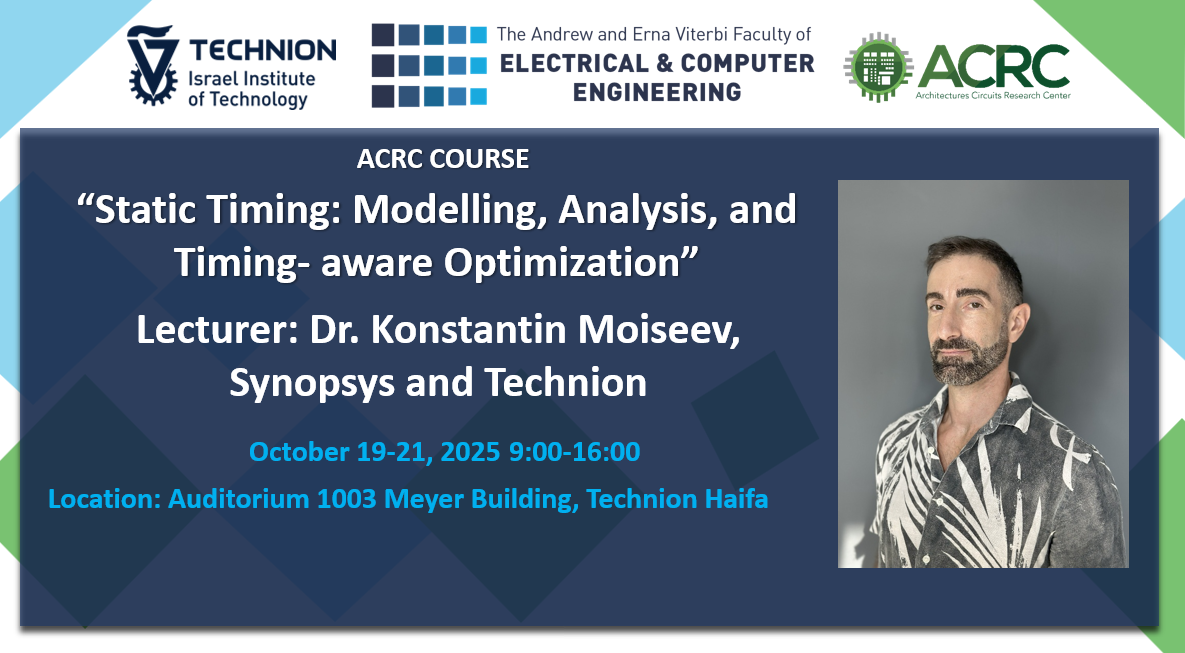
| Instructor: | Dr. Konstantin Moiseev, Synopsys and Technion |
| Teaching Assistant: | TBD |
| Lectures: | 3 days |
| Academic Points: | 1 |
| Exam: | TBD |
| Course Fees: | 1700$ (See membership options) |
For registration, click here
Registration closes on October 14, 2025
Date: October 19 – 21, 2025
Time: 9:00 – 16:00
Course Content:
In modern VLSI design, timing is everything. As technology continues to scale and performance demands increase, ensuring that a chip meets its timing requirements has become one of the most critical and complex challenges in digital design. Timing analysis and optimization have evolved significantly over the years, growing more intricate due to two major classes of effects associated with node scaling:
- Micro-level effects: These stem from emerging physical phenomena at the device or interconnect level, driven by shrinking feature sizes.
- Macro-level effects: These arise from the increasing complexity and size of circuits, enabled by the ability to integrate more logic onto a single die.
Addressing micro-level effects calls for novel modeling and analysis techniques, while macro-level challenges demand highly efficient algorithms to manage the escalating scale of timing analysis. Accurate timing analysis is essential to achieving fast and reliable timing closure. It must be integrated throughout the entire design flow—from high-level RTL and behavioral models, through logic synthesis and transistor-level optimization, to final layout—adapting to the available information at each stage. This course offers a comprehensive exploration of Static Timing Analysis (STA), blending foundational theory with practical, in-depth coverage of key topics, including:
- Interconnect and cell modeling
- Timing propagation
- Library characterization
- Constraint specification
- Variability and crosstalk effects
Additionally, the course provides a rare opportunity to delve into device-level STA, a topic often underrepresented in traditional VLSI education.
Course schedule:
Day 1
9:00 – 10:15: Introduction
- Importance of STA in the design flow
- STA vs. Simulation
- Structure of STA tool
- STA sub-topics – general overview
10:30 – 11:45 : Basic Concepts
- Delay / transition time definitions / abstractions
- Timing graph and timing arc
- Cell level / vs. device-level STA
13:00 – 14:15 & 14:30 – 16:00 : Device and interconnect modelling for timing
- MOSFET switching characteristics & intrinsic delay
- Parasitic capacitance / resistance / inductance
- Gate-level vs. transistor-level models. Library characterization.
- Linear delay models
- Non-linear delay models, NLDM
- Current Source Models (CCST, CCSN)
- Interconnect modelling, Elmore delay
- Moments, AWE
- Effective capacitance
Day 2
9:00 – 10:15: Constraints
- Timing checks
- FF vs. latch timing
- SDC, timing environment, input / output delays
10:30 – 11:45: Clocks
- Clock network
- Clock definitions and propagation
- Gated clocks
13:00 – 14:15 & 14:30 – 16:00: Path Analysis
- Timing graph
- Types of paths
- Arrival time, Required Time, Slack
- Critical path, N-worst paths
- Timing report analysis
- Special paths (multi-cycle, false, etc.)
- PBA vs. GBA
Day 3
9:00 – 10:15 & 10:30 – 12:00: Variation
- Sources of variation
- PVT – corner analysis
- Approaches to variation handling – OCV / AOCV / SOCV / POCV
- Statistical STA
- Characterization for variation
- Device vs. cell-level variation
- Monte-Carlo and correlation to Spice
13:00 – 14:15: Crosstalk and SI
- Fundamentals of capacitive noise
- Aggressor/victim analysis
- Models for peak noise/delay uncertainty. MCF. DCC
- Crosstalk-aware STA
14:30 – 16:30: Optimization
- Gate sizing by LR
- Buffer insertion
- ECO and incremental signoff
- Device-level optimization
For registration, click here