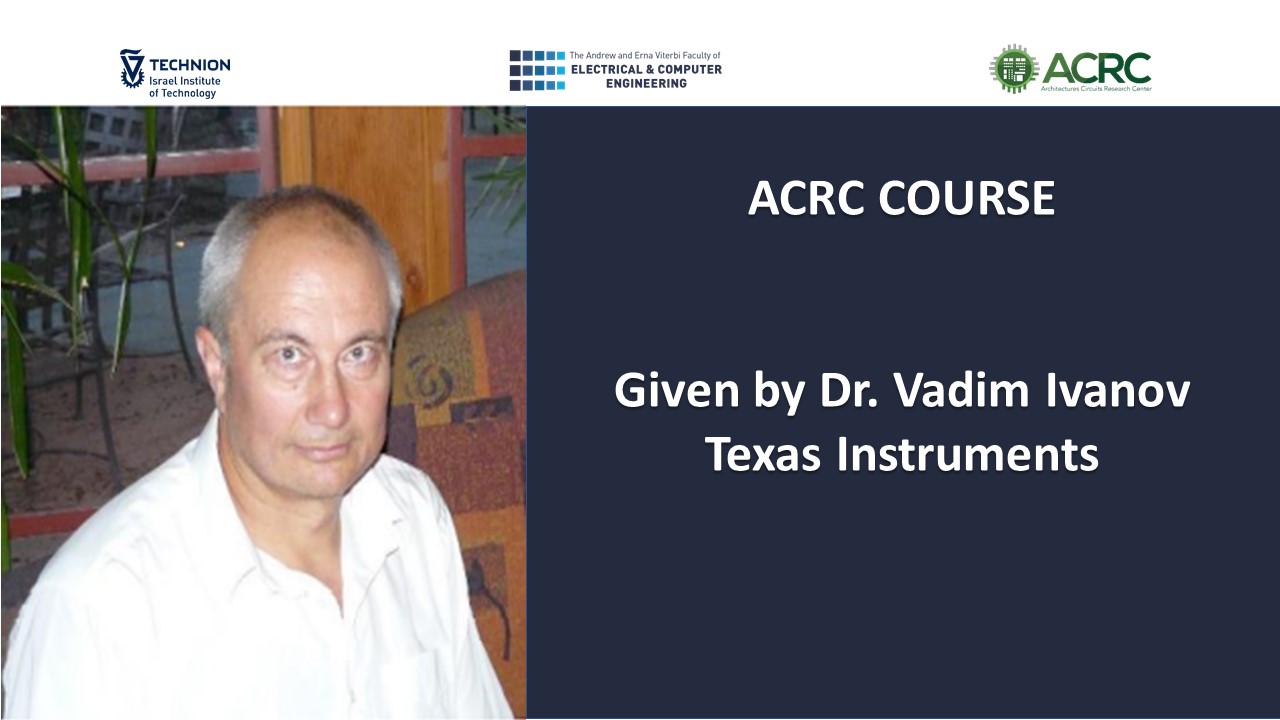
46954 – Accuracy Improvement of the Analog Integrated Circuits
February 26-28/2023, 9:00 a.m.
Auditorium 1003, Meyer Bld
Dr. Vadim Ivanov, Texas Instruments
| Instructor: | Vadim Ivanov |
| Teaching assistant: | Itamar Melamed |
| Lectures: | 13 hours, 3 days |
| Academic points: | 1pts |
| Exam: | TBD |
| Course Fee : | 1700$ (See membership options) |
*Registration is open until February 20, 2023
Course Content:
In 1951 Bernard Tellegen proved that set of an ideal amplifier, reference, limiter, and RC network
is functionally sufficient for the implementation of any analog functions. It has started a neverending quest to design ideal amplifiers and references. The most accurate voltage references use
the bandgap voltage of the silicon. Out of many options, the de facto standard of an ideal amplifier
is an operational amplifier. Operational amplifiers and bandgap voltage references have been the
first analog ICs in production (since the 1960-s), now with >20,000 types of such ICs available
from almost every semiconductor company and enjoying multi-billion sales just for stand-alone
ICs.
This course will start with an overview of the analog design methodology based on feedback
control of every important parameter in the system. While every feedback loop may be unstable,
we will demonstrate ways to verify and guarantee the stability of the resulting multiloop system.
This methodology will be illustrated with multiple non-trivial examples of current mirrors with
unmeasurable high output impedance; transconductors with wide input range, any load-stable
LDOs with instant load regulation.
Based on this methodology, we will proceed with the in-depth design of the bandgap voltage
references in different processes and for different applications. We will consider embedded
references in digital systems, references for the highest state-of-the-art accuracy, and references
with nanopower consumption. In addition to the circuit design and tradeoffs between
noise/consumption/settling time, we will discuss the challenges with testing, trimming, and
packaging.
The next part of the course is dedicated to improving all OpAmp parameters. These include
speed-to-power ratio, noise, CMRR and PSRR, and input and output voltage range. We will
consider offset and offset temperature drift trimming as well as structures and circuits for offset
elimination by auto-zeroing and chopping.
Topics per Day:
Day 1 (4 academic hours): Structural design methodology and
practical frequency compensation
Discussed are the rules of generating circuit solutions with desired analog functionality out of an
immense variety of options. Design starts with a graphic presentation of the problem with signal
flow graphs or block diagrams, then changing it to the form where everything necessary is
controlled with a dedicated feedback loop, and, finally, implementing the structure using an
elementary cell library. The resulting circuit comprises multiple feedback loops. Interaction
between these loops makes frequency compensation of such a system non-trivial task,
unsupported by the general control theory. Every MOS or bipolar transistor is nonlinear, which
may cause conditional stability and complicated compensation.
We will consider system structure design for stability, and additional elementary circuit cells to
the textbook set, resulting in achieving unconditional system stability when component
parameters vary, and when load and signal source impedance is not well defined.
Examples include LDOs stable with any load capacitance, transconductors with wide (few volts)
input voltage range, and multistage operational amplifiers.
Day 2 morning (2 academic hours): Bandgap voltage references
Discussed are error sources of the bandgap voltage references and techniques for improving their
accuracy: circuit techniques for low-noise bandgap generation core, feedback amplifier with
chopping offset elimination, output buffer with mOhm output impedance and fast settling on load
changes; single- dual and triple temperature trimming; packaging requirements; testing and
application particulars. Also presented circuit solutions for reverse bandgap reference,
operational from 0.9V supply, and reference structure and implementations with nanoampere
consumption.
Day 2 afternoon and Day 3 (7 academic hours): Operational amplifier
speed, accuracy, and consumption improvement
Discussed are circuit techniques to improve all essential parameters of the Operational Amplifiers.
Most circuit techniques shown have been previously published only in patents and applications.
Examples include input stage design for low offset, noise, unmeasurable PSRR and CMRR, input
common-mode voltage range; ways of improvement OpAmp speed to power ratio; open loop
gain; power supply range both in high- and low-voltage amplifiers; improving offset by a packagelevel trimming, auto-zero, and chopping; achieving high capacitive drive capability; current limit,
temperature protection, POR.
| 26FEB23 | 1 | 09:00 ~ 09:50 | Course Introduction, |
| 2 | 10:00 ~ 10:50 | Structural design methodology | |
| 3 | 11:00 ~ 12:00 | Structural design methodology | |
| 4 | 12:00 ~ 13:00 | Lunch Break | |
| 5 | 13:00 ~ 13:50 | Practical frequency compensation | |
| 6 | 14:00 ~ 15:15 | Practical frequency compensation | |
| 7 | 15:30 ~ 17:00 | Practical frequency compensation | |
| 8 | 17:10 ~ 18:00 | Q&A | |
| 27FEB23 | 1 | 09:00 ~ 09:50 | Bandgap voltage references |
| 2 | 10:00 ~ 10:50 | Bandgap voltage references | |
| 3 | 11:00 ~ 12:00 | Bandgap voltage references | |
| 4 | 12:00 ~ 13:00 | Lunch Break | |
| 5 | 13:00 ~ 13:50 | Operational amplifier speed, accuracy and consumption improvement | |
| 6 | 14:00 ~ 15:15 | Operational amplifier speed, accuracy and consumption improvement | |
| 7 | 15:30 ~ 17:00 | Operational amplifier speed, accuracy and consumption improvement | |
| 8 | 17:10 ~ 18:00 | Q&A | |
| 28FEB23 | 1 | 09:00 ~ 09:50 | Operational amplifier speed, accuracy and consumption improvement |
| 2 | 10:00 ~ 10:50 | Operational amplifier speed, accuracy and consumption improvement | |
| 3 | 11:00 ~ 12:00 | Operational amplifier speed, accuracy and consumption improvement | |
| 4 | 12:00 ~ 13:00 | Lunch Break | |
| 5 | 13:00 ~ 13:50 | Operational amplifier speed, accuracy and consumption improvement | |
| 6 | 14:00 ~ 15:15 | Operational amplifier speed, accuracy and consumption improvement | |
| 7 | 15:30 ~ 17:00 | Q&A | |
| 8 | 17:10 ~ 18:00 | Exam |
Prerequisites:
044137 Electronic Circuits
Recommended prerequisites:
046187 Analog Circuits Design
Grading:
Written exam – 100%
Instructor’s Bio:
MSEE 1980, Ph.D. 1987, both in the USSR. Designed electronic
systems and ASICs for naval navigation equipment from 1980 to
1991 in St. Petersburg, Russia and mixed signal ASICs for sensors,
GPS/GLONASS receivers and for motor control between 1991 and
1995.
Joined Burr Brown, now Texas Instruments, Tucson, in 1996, where
worked on the operational, instrumentation, power amplifiers,
references and switching and linear voltage regulators, and where
he is currently the Operational Amplifier Technologist. Has 126 patents, with more pending, on
analog circuit techniques and authored > 30 technical papers and three books: “Power Integrated
Amplifiers” (Leningrad, Rumb, 1987), “Analog system design using ASICs” (Leningrad, Rumb,
1988), both in Russian, and “Operational Amplifier Speed and Accuracy Improvement”, Springer,
2004
*Registration is open until February 12, 2023


