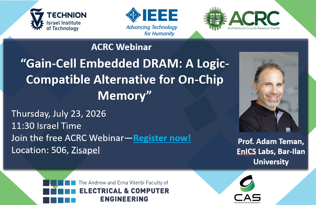
AI Data-center HW architecture

Instructor: Gil Bloch, NVIDIA Israel
Teaching Assistant: TBD
Lectures: 13 hours, 3 days
Academic Points: 1pts
Exam: TBD
Course Fees: 1700$ (See membership options)

For registration click here

*Registration is open until October 10, 2023

Course Content:

Artificial Intelligence, and specifically deep neural networks become the single most interesting application. It is expected that a growing percentage of the world’s compute power will be dedicated to training and inferencing of neural networks for many tasks.

Training large neural network models such as Large Language Models (LLM) require specialized systems and standard datacenters cannot train such models in an efficient way.

This course aim to cover multiple aspects of designing and building high-performance large-scale datacenters (supercomputers) for modern and future neural network training. In this course, we will cover accelerated computing and the role of GPUs and specialized CPUs in future AI systems as well as the importance of high-performance interconnect.

The course consists of a series of lectures. Several lectures are based on published papers and other cover recent research performed in NVIDIA.

This course aims at several categories of participants. Novice participants can learn about design tradeoffs and directions. Moreover, participants with high performance networking experience can update their knowledge and will be able to tune their experience to the state-of-the art.

Topics:

This course will cover advanced topic in supercomputer system architecture focusing on the interconnection between the compute engines, including interconnect hierarchies, communication algorithms and in-network computing.

Prerequisites:

Computer Architecture (046267 or 236267) and Networks and Internet (044334)

Schedule:

Day 1 (15/10/2023)

1.1. Introduction to supercomputing systems – 9:30-10:45

Coffee break – 10:45-11:15

1.2. Convergence of HPC and Cloud – 11:15-12:30

Lunch break – 12:30-13:30

1.3. Distributed AI training techniques – 13:30-14:45

Coffee break – 14:45-15:15

1.4. Distributed AI training techniques – 15:15-16:30

Day 2 (16/10/2023)

2.1. Challenges in modern distributed AI training (data reduction) – 9:30-10:45

Coffee break – 10:45-11:15

2.2. Challenges in modern distributed AI training (data reduction/all-to-all) – 11:15-12:30

Lunch break – 12:30-13:30

2.3. In-network computing (data reduction) – 13:30-14:45

Coffee break – 14:45-15:15

2.4. In-network computing (programmability) – 15:15-16:30

Day 3 (17/10/2023)

3.1. System topology considerations (NUMA, PCI, NVLink, Network) – 9:30-10:45

Coffee break – 10:45-11:15

3.2. Routing and congestion control – 11:15-12:30

Lunch break – 12:30-13:30

3.3. Fault tolerance – 13:30-14:45

Coffee break – 14:45-15:15

3.4. AI factories vs. AI in the cloud – 15:15-16:30

Bio:

Gil Bloch is an HPC and AI specialist with broad experience in fast interconnect technologies for clusters, datacenters and cloud computing. His current responsibilities include co-design and in-network computing for HPC and machine learning. Gil is a teacher of Fast Networks and RDMA programming in the Hebrew University of Jerusalem (HUJI) and in Ben Gurion University of the Negev (BGU).

Before working on in-network computing, Gil had multiple engineering and architecture positions including network adapters and switches ASIC design and architecture, RDMA offload ASIC and open-source networking software for high performance computing. Gil is an author/co-author of multiple patents in the area of computer networks and network adapters. Gil holds a BSc degree in Electrical Engineering from the Technion, Israel Institute of Technology.

Please leave your details here

*Registration is open till October 10, 2023

Mitigating Nonlinear Phenomena in Fractional-N Frequency Synthesis


Frequency synthesizers are universally used in a wide range of applications including clocking, communications, instrumentation, and radar. The most common architecture is the fractional-N frequency synthesizer which uses a nonlinear finite state machine to produce the desired frequency. Both the finite state machine itself and interaction between its output and nonlinearities in the implementation can lead to unwanted spurious periodic output frequency components (spurs) and excess noise. Understanding of the origins of these effects has led to the invention of novel mitigation strategies.

This talk will explain the underlying issues, explain some recent innovations, and highlight open problems.


Michael Peter Kennedy received the B.E. degree in electronics from the National University of Ireland, Dublin, the M.S. and Ph.D. degrees from the University of California, Berkeley, and the D.Eng. degree from the National University of Ireland. He has published and lectured on a range of topics in the field of nonlinear circuits and systems including oscillators, chaos, neural networks, mixed-signal testing, phase-locked loops, delta-sigma modulation and frequency synthesis. He was made an IEEE Fellow in 1998 for his contributions to the study of Neural Networks and Nonlinear Dynamics. He was awarded the IEEE Third Millennium Medal, the IEEE Circuits and Systems Society Golden Jubilee Medal, and the RIA Parsons Medal. He has held faculty positions at University College Cork, where he also served as Vice-President for Research and Innovation, and University College Dublin, where he is currently Professor of Microelectronic Engineering. He has had visiting appointments at BME, EPFL, Imperial College London, and the University of Pavia. He has provided consulting services to a number of semiconductor companies and was founding Director of Ireland’s Microelectronics Industry Design Association and the Microelectronic Circuits Centre Ireland. He served as President of the Royal Irish Academy from 2017 to 2020.

Important: participation is free of charge, but registration is required

For more details and updates on the series of “ACRC Semiconductor Webinars” please follow our newsletters and our website 

Let the Plants do the Talking: Smart Agriculture by the messages received from Plants and Soil

As reported in the report recently issued by the United Nations (Intergovernmental Panel on Climate Change – IPCC Report 2021), the benefits that technology provides to a green and sustainable economy are highly appreciated and under intense research and development globally. Circuits and Systems (CAS), which are the base for any system, can bring the needed functionalities and performances for reaching eco-friendly, circular, and practical solutions.

The IoT active connection in agriculture (as an example in Europe) are exponentially increasing, proving that Precision Agriculture is a very fast-growing research field, where more controlled quality production, water use optimization, and a lower spreading of pesticides and fertilizers are some key issues, serving the improvement of food quality, but also helping the respect of agriculture for the environment.

For reaching these targets, electronics are the perfect tool for interfacing the data sources, extracting the data and processing them, and obtaining the needed information along the whole food chain: from the farmer, and the professional stakeholders to the consumers.

In the Distinguished Lecture, an overview of electronics for precision agriculture will be presented, analyzing the possible solutions that can bring important innovations, advancing the actual strategies based on remote or indirect measurements, instead in-place measuring the plant and soil parameters (a.k.a. Let the Plants do The Talking), associated with more standard information derived from environmental conditions.

Application scenarios for crop monitoring, water control, information communication, and decision support will be presented. In particular, will be analyzed technologies for reaching the needed levels of low power and low cost, and the efficient ones to be applied to Agri-Food at the global scale, supporting also food security and sustainability.


Danilo Demarchi Full Professor at Politecnico di Torino, Department of Electronics and Telecommunications.

Micro&Nano Electronics, Smart System Integration, and IoTs for the Agri-Food Value Chain and for BioMedical Devices.

Visiting Professor at EPFL Lausanne (2019) and at Tel Aviv University (2018-2021).

Visiting Scientist (2018) at MIT and Harvard Medical School for the project SISTER (Smart electronic IoT SysTEms for Rehabilitation Sciences).

Author and co-author of 5 patents and more than 300 scientific publications in international journals and peer-reviewed conference proceedings.

Leading the MiNES (Micro&Nano Electronic Systems – http://mines.polito.it) Laboratory of Politecnico di Torino and coordinating the Italian Institute of Technology Microelectronics group at Politecnico di Torino (IIT@DET).

Founder and Editor in Chief of the IEEE Transactions on AgriFood Electronics – TAFE (https://ieee-cas.org/publication/ieee-transactions-agrifood-electronics).

Founder and General-Co-Chair of the IEEE Conference on AgriFood Electronics – CAFE (https://2023.ieee-cafe.org).

Founder and Vice-Chair of the IEEE CAS Special Interest Group on AgriFood Electronics.

2023-2024 Distinguished Lecturer for the IEEE CAS Society with the Lecture “Let the Plants Do the Talking: Smart Agriculture by the messages received from Plants and Soil”.

Member of the IEEE Sensors Council and the BioCAS Technical Committee. Associate Editor of the IEEE Open Journal on Engineering in Medicine and Biology (OJ-EMB).

General Chair of IEEE BioCAS (Biomedical Circuits and Systems) Conference in 2017 in Torino and founder of IEEE FoodCAS Workshop (Circuits and Systems for the FoodChain).

TPC Co-Chair of IEEE ICECS 2019, IEEE BioCAS 2021 and IEEE BioCAS 2022 conferences. General Co-Chair of IEEE BioCAS 2023.

Organizer of the 3rd Seasonal School on AgriFood Electronics: Smart Technologies for a Sustainable Agriculture in Torino, September 2022.


Important: participation is free of charge, but registration is required

For more details and updates on the series of “ACRC Semiconductor Webinars” please follow our newsletters and our website 


Emerging Building Blocks in Digital System-on-Chips


Instructor:  Mingoo Seok, Columbia University
Lectures:  3 days
Course Fee: 1700$ (See membership options)

*Registration is open until June 15, 2023

Schedule

Day 1 (19/6/23):

  1. SRAM-based in-memory computing (IMC) hardware
    1. Analog
    2. Digital
    3. IMC-based accelerator architecture

Day 2 (20/6/23):

  1. Analog mixed-signal computing
    1. Charge-based correlation calculation for GPS
    2. Analog signal processing for speech recognition
  2. Spike-based computing
  3. Spike neural network accelerator
  4. Divisive energy normalization in the spike domain

Day 3 (21/6/23):

  1. Digital LDO
  2. Metrics
  3. Recent techniques
  4. FoM and benchmark
  5. In-situ error detection and correction (EDAC)
  6. EDAC for setup timing error
  7. EDAC for metastability

Please leave your details

*Registration is open until June 15, 2023


Trans-impedance amplifiers design: from ultra-low-power analog to ultra-wideband RF

In this talk a few TIA design examples will be presented, covering different types of applications.

TIAs can be broadly grouped into two categories, i.e. closed-loop and open-loop topologies.

Closed loop TIAs generally have better frequency response precision and can achieve higher dynamic range, but typically have higher power dissipation and limited bandwidth.

Open loop topologies are preferred when very wide bandwidth or ultra-low power dissipations are required.

In wireless sensor networks or Internet-of-Things (IoT), bandwidth is limited but power dissipation is reduced to a minimum, leading to ultra-low-power TIAs that consume only a few uW.

In 5G FR1 receivers, TIAs with tens of MHz bandwidth and a very high dynamic range are required. Closed-loop architectures are dominant, often with complex op-amp architecture and with power consumptions in the order of a few mW.

In 5G FR2 receivers, TIAs with hundreds of MHz to a few GHz bandwidth are used, mostly based on open-loop topologies with power dissipations of tens of mW.


Danilo Manstretta Member, IEEE) received the Laurea degree (summa cum laude) and the Ph.D. degree in electrical engineering and computer science from the University of Pavia in 1998 and 2002, respectively.

From 2001 to 2003 he was with Agere Systems as a Member of the Technical Staff, working on WLAN transceivers and linear power amplifiers for base stations. From 2003 to 2005 he was with Broadcom Corporation, Irvine, CA, working on RF tuners for TV applications. In 2005 he joined the University of Pavia, where he is now an Associate Professor. His research interests are in the field of analog, RF, optical, and millimeter-wave integrated circuit design.

Dr. Manstretta has been a member of the Steering Committee of the IEEE Radio Frequency Integrated Circuits (RFIC) Symposium since 2017. He was a TPC member for the same conference from 2006 to 2021. He became TPC co-Chair in 2022 and is the RFIC TPC chair in 2023. He was Guest Editor of the IEEE Journal of Solid-State Circuits May 2017 Special Section dedicated to the 2016 RFIC Symposium and Guest Editor of the IEEE Transactions on Microwave Theory and Techniques June 2018 Mini Special Issue dedicated to the 2017 RFIC Symposium. He is a member of the European Solid-State Circuit Conference (ESSCIRC) TPC since 2022. He is a Distinguished Lecturer of the Solid-State Circuits Society. He was co-recipient of the 2003 IEEE Journal of Solid-State Circuits Best Paper Award.


Important: participation is free of charge, but registration is required

For more details and updates on the series of “ACRC Semiconductor Webinars” please follow our newsletters and our website 


Imaging in CMOS technologies using single-photon avalanche diodes

The ability to detect single photons with high sensitivity and precision is revolutionizing the image sensors field. Single-photon avalanche diodes (SPAD) not only are extremely sensitive, but they also retain with high accuracy the photon arrival time, which opens a whole new world of opportunities. Conventional image sensors circuitry is not anymore enough to manage this device, which requires a completely different readout chain.

In this lecture, an overview of the SPAD potential, with pros and cons, will be addressed. Typical circuit topologies employed in SPAD-based image sensors will be described, along with some examples of applications and current trends.


Matteo Perenzoni (M’09, SM’19) graduated in electronics engineering from the University of Padua, Italy, and received tPh.D. in Physics from the University of Ferrara, Italy.

In 2002, he collaborated with the University of Padua on mixed-signal integrated circuit design for channel decoding. In 2004, he joined the Fondazione Bruno Kessler (FBK), Trento, Italy, as a Researcher working at the Integrated Radiation and Image Sensors (IRIS) Research Unit. Meanwhile, he also taught courses on electronics and sensors at the Master and Doctorate School, University of Trento, Trento. In 2014, he was a Visiting Research Scientist with the THz Sensing Group, Microelectronics Department, TU Delft, The Netherlands. From 2017 to 2021 he led the IRIS Research Unit at FBK, working in the field of radiation and image sensors using custom and CMOS technologies. Since 2021 he is with the Sony Europe Technology Development Centre in Trento, Italy, leading the analog IC design team. His research interests include advanced CMOS image sensors with a focus on single-photon detection, THz image sensors, and optimization of analog integrated circuits.

Dr. Perenzoni has been a member of the Technical Program Committee of the European Solid-State Circuit Conference (ESSCIRC), from 2015 to 2021 and of the International Solid-State Circuit Conference (ISSCC) from 2018 to 2022.


Important: participation is free of charge, but registration is required

For more details and updates on the series of “ACRC Semiconductor Webinars” please follow our newsletters and our website 


On-chip communication: from architectures to circuits

On-chip communication directly impacts the performance, energy efficiency, and area of systems-on-chip, multi-processors, and highly-parallel accelerators, especially for emerging machine learning applications. In this talk, I will introduce a range of design options for on-chip interconnects, from point-to-point links to complex network topologies, starting from architecture to low-level circuit techniques. The presentation addresses base routing schemes and mapping of different protocol families, then moving on to microarchitecture, it presents flow-control and arbitration requirements and options. I will then detail circuit-level considerations, with a focus on different synchronization strategies across multiple clock domains, including multi-synchronous, source-synchronous-clocking, and fully-asynchronous circuits.


Yvain Thonnart received the MS degree from Ecole Polytechnique and an engineering diploma from Telecom Paris, France in 2005. He then joined the Technological Research Division of CEA, the French French Alternative Energies and Atomic Energy Commission, within the CEA-Leti institute until 2019, then within the CEA-List institute. He has led the development of several large research projects for on-chip communications, focusing on the maturation of novel concepts towards industrial adoption, such as communication between multiple voltage and frequency domains, 3D-stacked circuits, and optical on-chip interconnects, leading to more than 70 publications and 10 patents. He is now senior expert on communication and synchronization in systems on chip, and scientific advisor for the mixed-signal design lab. His main research interests include asynchronous logic, networks on chip, physical implementation, emerging technologies integration such as photonics, cryoelectronics and interposers. He is currently serving in the technical program committee of the ISSCC.


Important: participation is free of charge, but registration is required

For more details and updates on the series of “ACRC Semiconductor Webinars” please follow our newsletters and our website 


Accuracy Improvement of the Analog Integrated Circuits

46954 – Accuracy Improvement of the Analog Integrated Circuits

February 26-28/2023, 9:00 a.m.

Auditorium 1003, Meyer Bld


Dr. Vadim Ivanov, Texas Instruments

Instructor: Vadim Ivanov 
Teaching assistant: Itamar Melamed
Lectures: 13 hours, 3 days
Academic points: 1pts
Exam: TBD
Course Fee : 1700$ (See membership options)

For registration click here 

*Registration is open until February 20, 2023


Course Content:

In 1951 Bernard Tellegen proved that set of an ideal amplifier, reference, limiter, and RC network
is functionally sufficient for the implementation of any analog functions. It has started a neverending quest to design ideal amplifiers and references. The most accurate voltage references use
the bandgap voltage of the silicon. Out of many options, the de facto standard of an ideal amplifier
is an operational amplifier. Operational amplifiers and bandgap voltage references have been the
first analog ICs in production (since the 1960-s), now with >20,000 types of such ICs available
from almost every semiconductor company and enjoying multi-billion sales just for stand-alone
ICs.
This course will start with an overview of the analog design methodology based on feedback
control of every important parameter in the system. While every feedback loop may be unstable,
we will demonstrate ways to verify and guarantee the stability of the resulting multiloop system.
This methodology will be illustrated with multiple non-trivial examples of current mirrors with
unmeasurable high output impedance; transconductors with wide input range, any load-stable
LDOs with instant load regulation.
Based on this methodology, we will proceed with the in-depth design of the bandgap voltage
references in different processes and for different applications. We will consider embedded
references in digital systems, references for the highest state-of-the-art accuracy, and references
with nanopower consumption. In addition to the circuit design and tradeoffs between
noise/consumption/settling time, we will discuss the challenges with testing, trimming, and
packaging.
The next part of the course is dedicated to improving all OpAmp parameters. These include
speed-to-power ratio, noise, CMRR and PSRR, and input and output voltage range. We will
consider offset and offset temperature drift trimming as well as structures and circuits for offset
elimination by auto-zeroing and chopping.

Topics per Day:

Day 1 (4 academic hours): Structural design methodology and
practical frequency compensation
Discussed are the rules of generating circuit solutions with desired analog functionality out of an
immense variety of options. Design starts with a graphic presentation of the problem with signal
flow graphs or block diagrams, then changing it to the form where everything necessary is
controlled with a dedicated feedback loop, and, finally, implementing the structure using an
elementary cell library. The resulting circuit comprises multiple feedback loops. Interaction
between these loops makes frequency compensation of such a system non-trivial task,
unsupported by the general control theory. Every MOS or bipolar transistor is nonlinear, which
may cause conditional stability and complicated compensation.
We will consider system structure design for stability, and additional elementary circuit cells to
the textbook set, resulting in achieving unconditional system stability when component
parameters vary, and when load and signal source impedance is not well defined.
Examples include LDOs stable with any load capacitance, transconductors with wide (few volts)
input voltage range, and multistage operational amplifiers.
Day 2 morning (2 academic hours): Bandgap voltage references
Discussed are error sources of the bandgap voltage references and techniques for improving their
accuracy: circuit techniques for low-noise bandgap generation core, feedback amplifier with
chopping offset elimination, output buffer with mOhm output impedance and fast settling on load
changes; single- dual and triple temperature trimming; packaging requirements; testing and
application particulars. Also presented circuit solutions for reverse bandgap reference,
operational from 0.9V supply, and reference structure and implementations with nanoampere
consumption.
Day 2 afternoon and Day 3 (7 academic hours): Operational amplifier
speed, accuracy, and consumption improvement
Discussed are circuit techniques to improve all essential parameters of the Operational Amplifiers.
Most circuit techniques shown have been previously published only in patents and applications.
Examples include input stage design for low offset, noise, unmeasurable PSRR and CMRR, input
common-mode voltage range; ways of improvement OpAmp speed to power ratio; open loop
gain; power supply range both in high- and low-voltage amplifiers; improving offset by a packagelevel trimming, auto-zero, and chopping; achieving high capacitive drive capability; current limit,
temperature protection, POR.

26FEB23 1 09:00 ~ 09:50 Course Introduction,
2 10:00 ~ 10:50 Structural design methodology
3 11:00 ~ 12:00 Structural design methodology
4 12:00 ~ 13:00 Lunch Break
5 13:00 ~ 13:50 Practical frequency compensation
6 14:00 ~ 15:15 Practical frequency compensation
7 15:30 ~ 17:00 Practical frequency compensation
8 17:10 ~ 18:00 Q&A
27FEB23 1 09:00 ~ 09:50 Bandgap voltage references
2 10:00 ~ 10:50 Bandgap voltage references
3 11:00 ~ 12:00 Bandgap voltage references
4 12:00 ~ 13:00 Lunch Break
5 13:00 ~ 13:50 Operational amplifier speed, accuracy and consumption improvement
6 14:00 ~ 15:15 Operational amplifier speed, accuracy and consumption improvement
7 15:30 ~ 17:00 Operational amplifier speed, accuracy and consumption improvement
8 17:10 ~ 18:00 Q&A
28FEB23 1 09:00 ~ 09:50 Operational amplifier speed, accuracy and consumption improvement
2 10:00 ~ 10:50 Operational amplifier speed, accuracy and consumption improvement
3 11:00 ~ 12:00 Operational amplifier speed, accuracy and consumption improvement
4 12:00 ~ 13:00 Lunch Break
5 13:00 ~ 13:50 Operational amplifier speed, accuracy and consumption improvement
6 14:00 ~ 15:15 Operational amplifier speed, accuracy and consumption improvement
7 15:30 ~ 17:00 Q&A
8 17:10 ~ 18:00 Exam

Prerequisites:
044137 Electronic Circuits

Recommended prerequisites:
046187 Analog Circuits Design

Grading:

Written exam – 100%

Instructor’s Bio:

MSEE 1980, Ph.D. 1987, both in the USSR. Designed electronic
systems and ASICs for naval navigation equipment from 1980 to
1991 in St. Petersburg, Russia and mixed signal ASICs for sensors,
GPS/GLONASS receivers and for motor control between 1991 and
1995.
Joined Burr Brown, now Texas Instruments, Tucson, in 1996, where
worked on the operational, instrumentation, power amplifiers,
references and switching and linear voltage regulators, and where
he is currently the Operational Amplifier Technologist. Has 126 patents, with more pending, on
analog circuit techniques and authored > 30 technical papers and three books: “Power Integrated
Amplifiers” (Leningrad, Rumb, 1987), “Analog system design using ASICs” (Leningrad, Rumb,
1988), both in Russian, and “Operational Amplifier Speed and Accuracy Improvement”, Springer,
2004

For registration click here

*Registration is open until February 12, 2023


Circuits and technologies for implantable biomedical devices

Biological processes such as neuronal signaling and cell growth are among the most complex micro- and nano-scale processes in nature. Historically such processes have been studied at the system level because there were no tools available to study individual components of the process. However, cellular-level interfacing is needed to provide a better understanding of the brain and to develop more advanced prosthetic devices and brain-machine interfaces. With semiconductor technology innovations, much recent work has been focused on unraveling biological complexity, but also on driving new diagnoses, treatments, and therapies that are tailored to the individual. One of the drivers behind those innovations is novel CMOS circuits enabling multi-modal, high-precision data collection and analysis at ultra-low power consumption. In this talk, I will present recent biomedical developments based on silicon technology, and I will discuss the requirements, materials, circuit techniques, and design challenges of their ASIC and SoC platforms.


Carolina Mora Lopez received her Ph.D. degree in Electrical Engineering in 2012 from the KU Leuven, Belgium, in collaboration with imec, Belgium. From 2012 to 2018, she worked at imec as a researcher and analog designer focused on interfaces for neural-sensing applications. During this time, she was the lead analog designer and project leader of the Neuropixels development project which resulted in the conception and fabrication of the Neuropixels 1.0 and 2.0 neural probes. She is currently the principal scientist and team leader of the Circuits & Systems for Neural Interfaces team at imec, which develops circuits and technologies for electrophysiology, neuroprosthetics and BMI. Her research interests include analog and mixed-signal circuit design for sensor, bioelectronic and neural interfaces. Carolina is a senior IEEE member and serves on the technical program committee of the ISSC conference, ISSCC SRP, VLSI circuits symposium, and ESSCIRC conference.


Important: The participation is free of charge, but registration is required

For more details and updates on the series of “ACRC Semiconductor Webinars” please follow our newsletters and our website