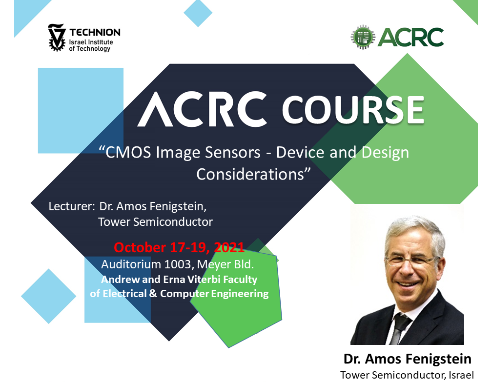
047003 – CMOS Image Sensors – Device and Design Considerations
October 17-19, 2021
Room 1003, Mayer Bld. Electrical Engineering Dept. Technion
Dr. Amos Fenigstein, Tower Semiconductors, Israel
Instructor: Dr. Amos Fenigstein
Teaching assistant: Shlomi Bouscher
Lectures: 13 hours, 3 days
Academic points: 1pts
Exam: 28.10.21, 14.30-16:30 and/or 25.11.21, 14.30-16:30
Topics
The course will cover image sensors (IS) principles, building blocks, characterization and optimization, including IS optics, device physics, performance parameters and advanced schemes.
Prerequisites
- (044231) Electron Devices 1 (MOS)
- (046237) Introduction to VLSI
- (044202) Stochastic Signals – recommended
Assignments
The course will consist of: lectures, self-practice exercises (25% of the grade), and a final exam (75% of the grade).
Course Abstract and Outline
This course deals with Image Sensors, starting with general requirements and specifications, sensor optics, image formation, resolution, Modulation Transfer Function (MTF), temporal and spatial noise, signal to noise ratio, and dynamic range. The course is focused on sensing devices, Charge Coupled Devices (CCD) and especially CMOS Image Sensors (CIS) where the modern CIS devices have CCDs-like components. The course especially emphasizes the Silicon device underlying the pixels. The course discusses in details the 3T and the 4T pixel technologies with buried, and with fully pinned (fully depleted) diodes. Different schemes of noise cancellation, advanced global shutter mode pixels and different schemes for wide dynamic range imaging will be discussed. There will be a short discussion on depth sensor based on time-of-flight (ToF) and the way they are implemented with CIS technology.
Course schedule:
17.10.21:
9:30-10:45 – Image Sensor Introduction – history and applications
10:45-11:15 – Coffee break
11:15-12:30 – Image Sensor optics, from scene to image, and image irradiance
12:30-13:30 – Lunch break
13:30-14:45 – Image Sensor optics – Chief Ray Angle (CRA) and microlens shift, Resolution and Modulation Transfer Function (MTF)
14:45-15:15 – Coffee break
15:15-16:30 – Semiconductor physics essentials, light absorption and its optimization
18.10.21:
9:30-10:45 – Device physics essentials, CIS pixel components
10:45-11:15 – Coffee break
11:15-12:30 – Pixel basics, the 3T pixel and its noise sources, pixel characterization
12:30-13:30 – Lunch break
13:30-14:45 – The kTC noise, noise suppression and cancellation
14:45-15:15 – Coffee break
15:15-16:30 – Modern image sensors – The pinned photodiode and the 4T pixel
19.10.21:
9:30-10:45 – Charge transfer –CCD principle, the buried CCD
10:45-11:15 – Coffee break
11:15-12:30 – Rolling and global shutter operation modes, and the shutter efficiency
12:30-13:30 – Lunch break
13:30-14:45 – High Dynamic Range Schemes
14:45-15:15 – Coffee break
15:15-16:30 – ToF sensors, iToF and dToF
Lecturer Bio
Dr. Fenigstein has been serving as Senior Director of R&D for Image Sensors since 2005. During these past years, his team has developed a wide range of CIS pixel technologies, from high-end cameras and industrial fast global shutter sensors, to large X-ray sensor and SPAD devices. Dr. Fenigstein has been with Tower since 2001 starting as device engineering manager. Before joining Tower, he managed a failure analysis team at Intel for its flip chip technology in the years 1998 – 2001. Prior to Intel, he worked for SCD on state-of-the-art MCT far infrared image sensors. Dr. Fenigstein received his B.Sc., M.Sc. and D.Sc. (Quantum Well IR sensors) in Electrical Engineering from the Technion – Israel Institute of Technology, where he currently lectures on CMOS and CIS technology.