“Bringing ML to the extreme edge: a story of co-optimizing processor architectures, scheduling and models” by Prof. Marian Verhelst

Deep neural network inference comes with significant computational complexity, making their execution until recently only feasible on power-hungry server or GPU platforms. The recent trend towards real-time embedded neural network processing on edge and extreme edge devices requires a thorough cross-layer optimization. The talk will analyze what impacts NN execution energy and latency. Subsequently, we will present different research lines of Prof. Verhelst’s lab exploiting and jointly optimizing NPU/TPU processor architectures, dataflow schedulers and conditional, quantized neural network models for minimum latency and maximum energy efficiency. This includes precision-scalable fully-digital designs, as well as compute-in-memory processors. Finally, this talk will make a case for more methodological design space exploration in the vast optimization space of embedded NN processors, using the ZigZag framework.

Marian Verhelst is a full professor at the MICAS laboratories of the EE Department of KU Leuven. Her research focuses on embedded machine learning, hardware accelerators, HW-algorithm co-design and low-power edge processing. Before that, she received a PhD from KU Leuven in 2008, was a visiting scholar at the BWRC of UC Berkeley in the summer of 2005, and worked as a research scientist at Intel Labs, Hillsboro OR from 2008 till 2011. Marian is a topic chair of the DATE and ISSCC executive committees, TPC member of VLSI and ESSCIRC  and was the chair of tinyML2021 and TPC co-chair of AICAS2020. Marian is an IEEE SSCS Distinguished Lecturer, was a member of the Young Academy of Belgium, an associate editor for TVLSI, TCAS-II and JSSC and a member of the STEM advisory committee to the Flemish Government. Marian currently holds a prestigious ERC Starting Grant from the European Union, was the laureate of the Royal Academy of Belgium in 2016, and received the André Mischke YAE Prize for Science and Policy in 2021.

Important: The participation is free of charge, but registration is required

/registration-marian-verhelst/

For more details and updates on the series of “ACRC Semiconductor Webinars” please follow our newsletters and our website

“CMOS Image Sensors – Device and Design Considerations “

047003 – CMOS Image Sensors – Device and Design Considerations

October 17-19, 2021

Room 1003, Mayer Bld. Electrical Engineering Dept. Technion

 Dr. Amos Fenigstein, Tower Semiconductors, Israel

Instructor:                    Dr. Amos Fenigstein

Teaching assistant:    Shlomi Bouscher

Lectures:                     13 hours, 3 days

Academic points:       1pts

Exam:                           28.10.21,  14.30-16:30  and/or  25.11.21, 14.30-16:30


Topics

The course will cover image sensors (IS) principles, building blocks, characterization and optimization, including IS optics, device physics, performance parameters and advanced schemes.

Prerequisites

  • (044231) Electron Devices 1 (MOS)
  • (046237) Introduction to VLSI
  • (044202) Stochastic Signals – recommended

Assignments

The course will consist of: lectures, self-practice exercises (25% of the grade), and a final exam (75% of the grade).

Course Abstract and Outline

This course deals with Image Sensors, starting with general requirements and specifications, sensor optics, image formation, resolution, Modulation Transfer Function (MTF), temporal and spatial noise, signal to noise ratio, and dynamic range. The course is focused on sensing devices, Charge Coupled Devices (CCD) and especially CMOS Image Sensors (CIS) where the modern CIS devices have CCDs-like components.  The course especially emphasizes the Silicon device underlying the pixels. The course discusses in details the 3T and the 4T pixel technologies with buried, and with fully pinned (fully depleted) diodes.  Different schemes of noise cancellation, advanced global shutter mode pixels and different schemes for wide dynamic range imaging will be discussed. There will be a short discussion on depth sensor based on time-of-flight (ToF) and the way they are implemented with CIS technology.

Course schedule:

17.10.21:

9:30-10:45 – Image Sensor Introduction – history and applications

10:45-11:15 – Coffee break

11:15-12:30 – Image Sensor optics, from scene to image, and image irradiance

12:30-13:30 – Lunch break

13:30-14:45 – Image Sensor optics – Chief Ray Angle (CRA) and microlens                                   shift, Resolution and Modulation Transfer Function (MTF)

14:45-15:15 – Coffee break

15:15-16:30 – Semiconductor physics essentials, light absorption and its                                      optimization

18.10.21:

9:30-10:45 – Device physics essentials, CIS pixel components

10:45-11:15 – Coffee break

11:15-12:30 – Pixel basics, the 3T pixel and its noise sources, pixel characterization

12:30-13:30 – Lunch break

13:30-14:45 – The kTC noise, noise suppression and cancellation

14:45-15:15 – Coffee break

15:15-16:30 – Modern image sensors – The pinned photodiode and the 4T pixel

19.10.21:

9:30-10:45 – Charge transfer –CCD principle, the buried CCD

10:45-11:15 – Coffee break

11:15-12:30 – Rolling and global shutter operation modes, and the shutter                                    efficiency

12:30-13:30 – Lunch break

13:30-14:45 – High Dynamic Range Schemes

14:45-15:15 –  Coffee break

15:15-16:30 – ToF sensors, iToF and dToF

Lecturer Bio

Dr. Fenigstein has been serving as Senior Director of R&D for Image Sensors since 2005. During these past years, his team has developed a wide range of CIS pixel technologies, from high-end cameras and industrial fast global shutter sensors, to large X-ray sensor and SPAD devices. Dr. Fenigstein has been with Tower since 2001 starting as device engineering manager. Before joining Tower, he managed a failure analysis team at Intel for its flip chip technology in the years 1998 – 2001.  Prior to Intel, he worked for SCD on state-of-the-art MCT far infrared image sensors. Dr. Fenigstein received his B.Sc., M.Sc. and D.Sc. (Quantum Well IR sensors) in Electrical Engineering from the Technion – Israel Institute of Technology, where he currently lectures on CMOS and CIS technology.

“Digital Predistortion for 5G MIMO Transmitters Using Machine Learning”

Digital predistortion (DPD) has been widely adopted to keep RF power amplifier operating with high efficiency without losing linearity in the exiting 4G systems. It is expected that DPD will continue to be deployed in 5G systems.  However, due to shifting from the single antenna to the multiple-input multiple-output (MIMO) phased array and continuously increased signal bandwidth, system designers face significant challenges in managing power consumption and meeting linearity requirement of  wireless  transmitters.  In this talk, we will discuss how the recently developed machine learning techniques can be utilised to resolve some of the issues in linearizing 5G MIMO systems, including data-clustering assisted DPD for multiple dynamic configurations, model tree-based behavioural model construction and simplified model extraction techniques.

Anding Zhu received the Ph.D. degree in electronic engineering from University College Dublin (UCD), Dublin, Ireland, in 2004. He is currently a Professor with the School of Electrical and Electronic Engineering, UCD. His research interests include high-frequency nonlinear system modeling and device characterization techniques, high-efficiency power amplifier design, wireless transmitter architectures, digital signal processing, and nonlinear system identification algorithms. He has published more than 160 peer-reviewed journal and conference articles. Professor Zhu served as the Secretary of Administrative Committee (AdCom) of IEEE Microwave Theory and Techniques Society (MTT-S) in 2018. He is currently an Elected Member of MTT-S AdCom, the Chair of Electronic Information Committee and the Vice Chair of Publications Committee. He is also the Chair of MTT-S Microwave High-Power Techniques Committee and a Track Editor of IEEE Transactions on Microwave Theory and Techniques.

Important: The participation is free of charge, but registration is required

/registration-anding-zhu/

For more details and updates on the series of “ACRC Semiconductor Webinars” please follow our newsletters and our website

“Cryo-CMOS electrical interfaces for large-scale quantum computers” by Prof. Fabio Sebastiano

Quantum computers operate by processing information stored in quantum bits (qubits), which must typically operate at cryogenic temperature. Today the qubits are mostly controlled by conventional electronics working at room temperature. This thermal gap can be readily bridged by a few wires since today’s quantum computers employ only a few qubits. However, practical quantum computers will require more than thousands of qubits, making this approach impractical. A more scalable approach requires operating a complex electronic interface at cryogenic temperature, very close to the quantum processor, eventually in the same package or even on the same chip. Thanks to its high integration capabilities, CMOS is the most viable technology for such a cryogenic interface. In this talk, we will first review the functionalities required to drive and control the most popular qubit technologies, and the requirements on the performance of the electronics. Based on those requirements and the behavior of CMOS devices at cryogenic temperature, several state-of-the-art cryo-CMOS circuits and systems have been designed, both for qubit drive and readout, and we will show their verification with real-world qubits, highlighting challenges and opportunities. Finally, the prospects towards large-scale quantum computers will be outlined, and we will try to answer the questions: Is the electronics a bottleneck for future quantum computers? How will we design cryo-CMOS circuits to tackle this challenge?

Fabio Sebastiano received the B.Sc. (cum laude) and M.Sc. (cum laude) degrees in electrical engineering from University of Pisa, Italy, in 2003 and 2005, respectively, the M.Sc. degree (cum laude) from Sant’Anna school of Advanced Studies, Pisa, Italy, in 2006 and the Ph.D. degree from Delft University of Technology, The Netherlands, in 2011.

From 2006 to 2013, he was with NXP Semiconductors Research in Eindhoven, The Netherlands, where he conducted research on fully integrated CMOS frequency references, nanometer temperature sensors, and area-efficient interfaces for magnetic sensors. In 2013, he joined Delft University of Technology, where he is currently an Associate Professor and the Research Lead of the Quantum Computing Division of QuTech. He has authored or co-authored one book, 11 patents, and over 80 technical publications. His main research interests are cryogenic electronics, quantum computing, sensor read-outs, and fully integrated frequency references.

Important: The participation is free of charge, but registration is required

/registration-fabio-sebastiano/

For more details and updates on the series of “ACRC Semiconductor Webinars” please follow our newsletters and our website

“Power efficiency in the next generation of 5G-6G analog front-ends” by Prof. Antonio Liscidini

Nowadays, both digital and analog electronics are reaching fundamental limits that will require revolutionary approaches to satisfy the power/bandwidth requirements of the next generation of data-driven applications.

After a brief overview of the modern wireless transceiver architecture, some key elements that will characterize 5G and 6G networks will be discussed. The talk will continue by analyzing the power efficiency of the analog signal processing by highlighting the presence of a thermodynamic upper-bound which relates dynamic range, bandwidth and power dissipation. Alternative strategies to circumvent this limit will be discusses such as adaptivity, passive time-variant signal processing and quantized analog signal processing. In particular, the latter represents a novel approach where the analog and digital domain are fused together in a more fluid scenario compared to traditional mixed-signal circuits. This operation leads to superior power efficiency and flexibility.

The effectiveness of the proposed solutions will be demonstrated through simulations and measurement results on different prototypes.

Antonio Liscidini received the Laurea (summa cum laude) and Ph.D. degrees in electrical engineering from the University of Pavia, Pavia, Italy, in 2002 and 2006, respectively.

He was a summer Intern with National Semiconductors, Santa Clara, CA, USA, in 2003, studying poly phase filters and CMOS low-noise amplifiers. From 2008 to 2012, he was an Assistant Professor with the University of Pavia and a consultant with Marvell Semiconductors, Pavia, in the area of integrated circuit. In 2012, he moved to the Edward S. Rogers Sr. Department of Electrical and Computer Engineering, University of Toronto, Toronto, ON, Canada, where he is currently an Associate professor. In 2019 he has become consultant for Huawei Technology Group in the area of RFIC for optical communication. His research interests are focused on analog mixed signal interfaces with particular emphasis on the implementations of transceivers and frequency synthesizers for wireless and wireline communication.

Dr. Liscidini was a recipient of the Best Student Paper Award at the IEEE 2005 Symposium on VLSI Circuits and co-recipient of the Best Invited Paper Award at the 2011 IEEE CICC and the Best Student Paper Award at the 2018 IEEE ESSCIRC. He has served as an Associate Editor for the IEEE Transactions on Circuits and Systems II: Express Briefs (2008-2011) (2017- 2018) and for the IEEE Open Journal of Solid-State Circuit Society (2021), as a Guest Editor for the IEEE Journal of Solid-State Circuits (2013) (2016) and Guest Editor of the IEEE RFIC Virtual Journal (2018). He has been member of the ISSCC TPC (2012- 2017), of the ESSCIRC TPC (2010-2018), and of the CICC TPC (2019-currently). Between 2016 and 2018, he has been a Distinguished Lecturer of the IEEE Solid-State Circuits Society.

Important: The participation is free of charge, but registration is required

/registration-antonio-liscidini/

For more details and updates on the series of “ACRC Semiconductor Webinars” please follow our newsletters and our website

“Embedded Systems Design in the Era of AI” by Prof. Michael Huebner

The increasing demands of complexity, flexibility and self-organization of networked embedded systems require new solutions for the local processor architectures and firmware. This includes the ability to adapt to the requirements of an algorithm e.g. in relation to a sensor value measured by an Cyberphysical System. Artificial intelligence becomes ubiquitous and therefore enters also the domain of embedded systems and enables enormous opportunities in edge computing. This will introduce new degrees of freedom in embedded and Cyberpyhsical systems and is very promising to support the aforementioned demands tremendously. In this talk, possible solutions for next generation embedded systems with AI components will be introduced.

Michael Huebner is a Full Professor and leads the Chair for Computer Engineering at the Brandenburg University of Technology (BTU) in Cottbus, Germany, since 2018.

He is also Vice-President for research and transfer at BTU since December 2020.

He received his diploma degree in electrical engineering and information technology in 2003, his Ph.D. degree in 2007 from the University of Karlsruhe (TH), and did his habilitation in 2011 at the Karlsruhe Institute of Technology (KIT) in the domain of reconfigurable computing systems.

His research interests are in reconfigurable computing and particularly new technologies for adaptive FPGA run-time reconfiguration and on-chip network structures with application in automotive systems, incl. the integration into high-level design and programming environments.

Important: The participation is free of charge, but registration is required

/registration-michael-huebner/

For more details and updates on the series of “ACRC Semiconductor Webinars” please follow our newsletters and our website

“An Organic-Photoconductive-Film CMOS Image Sensor’s Advanced Technologies” by Kazuko Nashimura

We have developed a CMOS image sensor with an organic photoconductive film (OPF) laminated on pixel circuits, different from those of a conventional silicon image sensors, in which the organic thin film for photoelectric conversion and the charge storage part for signal charge accumulation are completely independent. In this presentation, we focus on the advantageous features of the OPF image sensor; [1] technology that realizes over 120 dB simultaneous-capture wide dynamic range; [2] global shutter technology achieving high saturation signals per unit square that is 10 dB higher than that of silicon image sensors with the global shutter function, without sacrificing pixel area; [3] RGB-NIR sensor technology capable of controlling NIR sensitivity by simply controlling the voltage applied to the OPF. Moreover, we introduce about 8K4K high resolution sensor technologies with 60fps high frame rate, 450ke- high saturation signals, and the global shutter function at the same time. We believe these features of the OPF image sensor will contribute to leaps in the imaging and sensing fields.

Kazuko Nishimura received the B.E. degree in mechanical engineering from Osaka University, and joined Panasonic Corporation where she engaged in high-speed analog-to-digital converters (ADCs) in 1995. She developed optical communication systems for fiber-to-the-home (FTTH), RF tuners and CMOS image sensors. Currently, she is a manager in Technology Division (R&D Division), Panasonic Corporation and pursues research on the organic photoconductive film (OPF) CMOS image sensors and sensor applications. She serves A-SSCC data converter subcommittee chair and ISSCC Imagers, Medical, MEMS and Displays subcommittee, IEEE SSCS distinguished Lecturer, and the SSCS Adcom. She is a senior member of IEEE.

Important: The participation is free of charge, but registration is required

/registration-kazuko-nishimura/

For more details and updates on the series of “ACRC Semiconductor Webinars” please follow our newsletters and our website


Introduction to Digital Radio Frequency Circuit Design”

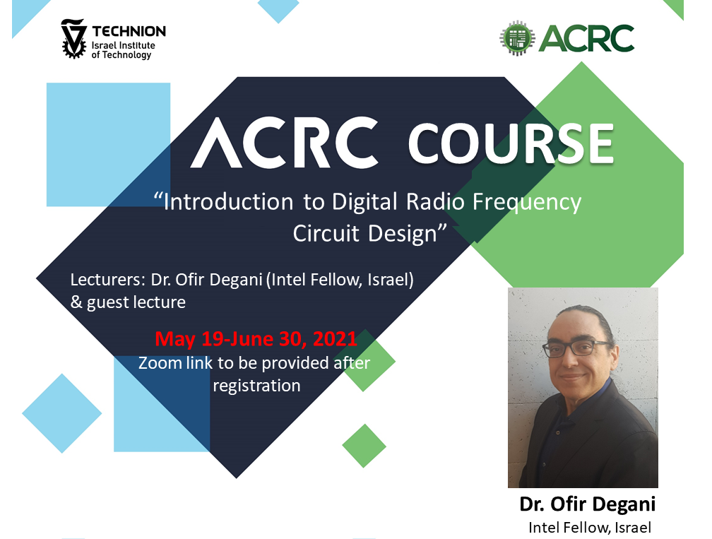
May 19-June 30, 2021, Zoom

Instructor:                    Dr. Ofir Degani and guest lecturers from Intel

Teaching assistant:   Itamar Melamed (itamar.m@campus.technion.ac.il )

Lectures:                       26 hours, 6 weeks.

Academic points:       2pts

Exam:                             final project


Topics

The course will cover the operation principles and the design of modern digital radio frequency circuit topologies and system architectures with enhanced digital signal processing.

Prerequisites

  • Linear Electronic Circuits (044142) or Electronic Circuits (044137)
  • Receiving and Transmitting Techniques (044214) or RFIC (046903)

Assignments

The course will consist of: lectures, discussion, practical examples, and a final project.

The grade will be based on quizzes (30%) and the final project (70%).

The individual projects will include a transistor level schematic design project of a selected circuit based on the course topics (e.g., TDC, DTC) according a required specifications. The project will be mentored by the course guest lecturers. The project options will be published during the course.

A 30 min presentation (followed by 10 min for questions) of the project is expected covering the project goals, design methodologies used, and simulation results. The grade will be set by a committee of the course staff and the guest lecturers reviewing the presentation.

Course Abstract and Outline

The increasing demand for over-the-air data traffic imposes requirements for wireless protocols and transceivers to support wider (e.g., 160 MHz) channel bandwidths, higher order modulation schemes (e.g., 1k-QAM OFDM), and MIMO and multilink schemes to allow for the increased wireless throughput. As many wireless enabled devices are battery powered and mobile, there is also a continuous demand to improve power consumption, cost, and form factor. Reducing the power dissipation becomes even more critical with the simultaneous operation of multiple chains.

These trends have driven higher levels of integration of the radio, with digital SoCs, on advanced CMOS processes. However, implementing the transceiver on a deeply scaled process node presents major challenges from having to operate off low supply voltages. In addition, traditional RF designs require accurate transistor and passive models, which can become a time-to-market limitation for the whole SoC.

As a result, in recent years, there has been a shift in wireless transceivers toward digital radio architectures due to their more compact die area, scalability in advanced CMOS processes, and the improved power efficiency. Furthermore, digital circuit topologies open paths to include digital processing algorithms that can enhance the circuit capabilities beyond the traditional analog designs allow. Examples for such topologies include digital phase lock loops and digital transmitters that will be explored.

The course discusses the operation principles and the design of modern digital radio frequency circuit topologies and system architectures with enhanced digital signal processing. Two main examples will be presented and discussed in detail, the first of digital phase lock loops and the second of digital transmitters. Their basic operation principles and modeling will be discussed and compared to the equivalent analog radio components.

Course schedule:

19.05.21 Dr. Ofir Degani – 17:00-19:00

Introduction to Digital Radio Frequency Transmit and Receive (RF-TRX) circuits. Comparison vs. Analog RF-TRX, motivations, examples from literature

24.05.21: Dr. Evgeny Shumaker – 17:00-19:00

Introduction to phase lock loops (PLL), basic structure and operation principles of Analog PLL and Digital PLL. DPLL model and jitter/phase noise budgets – Part 1

26.05.21: Dr. Evgeny Shumaker – 17:00-19:00

Introduction to phase lock loops (PLL), basic structure and operation principles of Analog PLL and Digital PLL. DPLL model and jitter/phase noise budgets – Part 2

31.05.21: Rotem Banin – 17:00-19:00

Introduction to Time to Digital Converters (TDC), resolution, noise and meta stability, flash TDC, Vernier TDC, interpolating TDC & stochastic TDC, Part 1

02.06.21: Rotem Banin – 17:00-18:00

Introduction to Time to Digital Converters (TDC), resolution, noise and meta stability, flash TDC, Vernier TDC, interpolating TDC & stochastic TDC, Part 2

07.06.21: Run Levinger – 17:00-19:00

Introduction to Digitally Controlled Oscillators, frequency resolution, noise modeling – Part 1

09.06.21: Run Levinger – 17:00-18:00

Introduction to Digitally Controlled Oscillators, frequency resolution, noise modeling – Part 2

14.06.21: Assaf Ben-Bassat – 17:00-19:00

Introduction to RF Transmitters (TX), basic structure and operation principles of Analog TX (ATX) and Digital TX (DTX). Types of digital transmitters and their working principles: quadrature DTX, 2 point polar DTX, DTC based polar DTX

16.06.21: Elan Banin – 17:00-19:00

DTX signal generation Digital front end (DFE), non regular time sampling: FSRC, zero crossing algorithms

17.06.21: Shahar Gross – 17:00-19:00

Basic performance indicators for digital TX chains and impairments. Pre-distortion techniques

21.06.21: Dr. Gil Asa – 17:00-19:00

Introduction to digital to time converters (DTC) and operation principles. DTC architectures segmentation, coarse phase modulators (MUX based, multi modulus divider based), fine phase modulators (delay based, interpolation based). Non idealities and non linearities – Part 1

23.06.21: Dr. Gil Asa – 17:00-19:00

Introduction to digital to time converters (DTC) and operation principles. DTC architectures segmentation, coarse phase modulators (MUX based, multi modulus divider based), fine phase modulators (delay based, interpolation based). Non idealities and non linearities – Part 2

28.06.21: Dr. Ashoke Ravi – 17:00-19:00

Introduction to digital power amplifiers (DPA) and operation principles. Current mode RF DAC/DPA vs. capacitive mode RF DAC/DPA – Part 1

30.06.21: Dr. Ashoke Ravi – 17:00-19:00

Introduction to digital power amplifiers (DPA) and operation principles. Current mode RF DAC/DPA vs. capacitive mode RF DAC/DPA – Part 2

Lecturer Bio

Ofir Degani (Senior Member, IEEE) has received the B.Sc. degree (summa cum laude) in electrical engineering and the B.A. degree in physics (summa cum laude) and the M.Sc. and Ph.D. degrees all from the Technion—Israel Institute of Technology, Haifa, Israel, in 1996, 1999, and 2005, respectively. His Ph.D. research was on MEMS inertial sensors and electrostatic actuators.

He joined the Mobility Wireless Group, Intel Corporation, Haifa, in 2006. His recent research interest includes integrated transceivers, digital transmitters, and mmWave radios in CMOS technology. He has authored or coauthored more than 80 journal articles and conference papers. He has filed more than 50 patents.

Dr. Degani was a recipient of the prestigious 2002 Graduate Student Fellowship from the IEEE Electron Devices Society and the Charles Clore Scholarship at the Charles Clore Foundation.

Guest Lecturers Bios

Assaf Ben-Bassat (Member, IEEE) received the B.Sc. and M.Sc. degrees in electrical engineering from the Technion—Israel Institute of Technology, Haifa, Israel, in 1997 and 2001, respectively, with a focus on the field of electro-optics.

From 2001 to 2003, he was with All-Optical, Haifa, developing lasers for high-speed optical communications. He joined Intel Corporation, Haifa, in 2003, where he develops circuits for baseband, RF, PLLs, and LO generation and distribution.

Shahar Gross received the B.Sc. degree in physics and the B.Sc. and M.Sc. degrees in electrical engineering from Tel Aviv University, Tel Aviv, Israel, specializing in signal processing, communication, and information theory.

In 2012, he joined as a PHY System Engineer with the Wireless Products Division, Intel Corporation, Petach-Tikva, Israel, where he is currently a PHY architect and is focused on advanced transmitter features. He took part in the Wi-Fi 6 standardization process and led the Wi-Fi PHY architecture of Intel’s first Wi-Fi 6 product.

Elan Banin received the B.Sc. degree in mechanical engineering from Tel Aviv University, Tel Aviv, Israel, in 2006.

He joined Intel Corporation, Petach-Tikva, Israel, in 2010, where he has worked as a DSP and Algorithms Engineer on multiple communication technologies.

Rotem Banin received the B.Sc. degree in electrical engineering from the Technion—Israel Institute of Technology, Haifa, Israel, in 2006, and the M.Sc. degree from Tel Aviv University, in 2015, Israel.

He joined the Mobility Wireless Group, Intel Corporation, Haifa in 2003. His recent research interest includes high-speed mixed-signal circuits and systems, integrated transceivers, digital transmitters, digital PLLs, and serial interfaces.

Ashoke Ravi (Senior Member, IEEE) received the B.Tech. degree in electrical engineering from IIT Madras, Chennai, India, and the M.S. and Ph.D. degrees in electrical and computer engineering from Carnegie Mellon University, Pittsburgh, PA, USA.

In 2001, he joined Intel Corporation, Hillsboro, OR, USA, where he is currently a Principal Engineer, working on innovation projects with the Advanced Radio Technology Team. His prior contributions were in developing integrated RF transceivers on deeply scaled CMOS processes and MIMO radios. He has authored or coauthored 50 IEEE conference papers and journal articles and coauthored three book chapters. He has 35 issued patents in this field. His research interests are in RF and mixed-signal circuits and architectures for connectivity, cellular, and SoC applications. Over the last several years, these activities have included leading the research and development of mm-waveband transceivers, digital polar and outphasing transmitters, digital PLLs, and data converters.

Dr. Ravi was nominated to the MIT Technology Review’s list of top 35 young innovators (the TR35) in 2009.

Gil Asa (Ph.D.) has received B.Sc. , M.Sc. , Ph.D. (all summa cum laude, from the Technion -IIT), focusing on micro-electronics. He graduated Ph.D. at 1999 researching advanced nuclear camera and detectors. At 1998 he took part in the Technion Israeli satellite project with design of Gamma ray spectrometer, which reports supernova activities. Till 2002 he was a project leader at IBM research labs working on ultra-high speed SiGe serializers, and till 2006 he was a senior circuit designer at Marvell working on self-invented digital PLL. Till 2012 he was the founder and CTO of compact SRAM start up and till 2015 he was an analog expert consultant at Inomize, working on video camera implanted inside the eye of partially blind patients. Since 2015 he joined Intel as signal integrity leader and since 2017 the focus is on RF circuit design, digital transmitters and relevant IP development. Dr. Asa has at least 10 academic papers, and over 25 worldwide patents (10 of them as sole inventor).

Run Levinger received the M.Sc. degree (Summa Cum Lauda) in electrical and electronics engineering from Tel-Aviv University, Tel Aviv, Israel, in 2015. His research thesis focused on linearization techniques for integrated E-band transmitter circuits such as up-converting mixers and power detectors. In 2011, he joined the IBM Haifa Research Laboratories, Haifa, Israel, where he was a Research Staff Member with the mm-Wave Technologies Group. In 2016, he joined Intel’s Radio Product Development group, Petah-Tikva, Israel, where he is a senior technical staff member. His research interests include designing, measuring, and modeling of integrated RF and millimeter-wave voltage and digital controlled oscillators (VCOs and DCOs), frequency synthesizers, frequency dividers, mixers, power detectors, and passives

for communication, radar, and imaging applications. He has Authored and Co-Authored more than 25 Conference and Journal papers and holds 10 US patents with several more pending.

Evgeny Shumaker graduated B.Sc. (summa cum laude), M.Sc. (summa cum laude) and Ph.D. degrees all from the Electrical Engineering department, Technion—Israel Institute of Technology, Haifa, Israel, in 2002, 2004, and 2010, respectively. His Ph.D. dissertation focused on basic limits and applications of slow and fast light phenomenon in microwave photonics.

In 2010 he joined IBM Haifa Research Laboratory where he was a Research Staff Member, leading R&D of passive millimeter wave imaging systems. In 2015 he joined Intel’s Radio Product Development group, Haifa, Israel, where he is currently a Senior Technical Staff Member. His research interests include real-time algorithms and techniques for high precision digital frequency synthesis. He has authored or coauthored more than 40 journal articles and conference papers and filed more than 10 patents.

Dr. Shumakher is a two-time recipient of the E.I. Jury award (2004, 2009) and the prestigious Graduate Student Fellowship from the IEEE Photonics Society (2009).

“Hardware Security and Safety of IC Chips” webinar by Prof. Makoto Nagata

IC chips are key enablers to a smartly networked society and need to be more compliant to security and safety. For example, semiconductor solutions for autonomous vehicles must meet stringent regulations and requirements. While designers develop circuits and systems to meet the performance and functionality of such products, countermeasures are proactively implemented in silicon to protect against harmful disturbances and even intentional adversarial attacks.

This talk will start with Electromagnetic Compatibility (EMC) techniques applied to IC chips for safety to motivate EMC-aware design, analysis, and implementation. It will discuss IC design challenges to achieve higher levels of hardware security (HWS). Crypto-based secure IC chips are investigated to avoid the risks of side-channel leakages and side-channel attacks, corroborated with silicon demonstrating analog techniques to protect digital functionality. The EMC and HWS disciplines derived from electromagnetic principles are key to establishing IC design principles for security and safety.

Makoto Nagata received the B.S. and M.S. degrees in physics from Gakushuin University, Tokyo, in 1991 and 1993, respectively, and a Ph.D. in electronics engineering from Hiroshima University, Hiroshima, in 2001.. He is currently a professor of the graduate school of science, technology and innovation, Kobe University, Kobe, Japan. He is a senior member of IEICE and IEEE.

His research interests include design techniques targeting high-performance mixed analog, RF and digital VLSI systems with particular emphasis on power/signal/substrate integrity and electromagnetic compatibility, testing and diagnosis, three-dimensional system integration, as well as their applications for hardware security and safety.

Dr. Nagata has been a member of a variety of technical program committees of international conferences. He is chairing the Technology Directions subcommittee for International Solid-State Circuits Conference (2018-present). He is also serving as SSCS AdCom member since 2020. He is currently an associate editor for IEEE Transactions on VLSI Systems (2015-present).

Important: The participation is free of charge, but registration is required

http://registration-makoto-nagata

For more details and updates on the series of “ACRC Semiconductor Webinars” please follow our newsletters and our website

“Asynchronous Stream Computing for Low Power IoT – Asynchronous Stochastic Computing (ASC), Asynchronous Stream Processing (ASP) and Asynchronous Impulse Radio (AIR) for ubiquitous sensing at the Edge” webinar by Prof. Mircea R. Stan

Asynchronous circuits have many potential advantages over their synchronous counterparts in terms of robustness to parameter variations, wide supply voltage ranges, and potentially low power by not needing a clock, yet their promise has not been translated yet into commercial success due to several issues related to design methodologies and the need for handshake signals. Stochastic computing is another processing paradigm that has shown promises of low power and extremely compact circuits but has yet to become a commercial success mainly because of the need for a fast clock to generate the random streams.
In this talk we will go over three complementary circuit techniques: Asynchronous Stochastic Computing (ASC), Asynchronous Stream Processing (ASP) and Asynchronous Impulse Radio (AIR). These techniques combine the best features of asynchronous circuits with the best features of stochastic computing to enable extremely compact and low power IoT sensing nodes. Together they can fulfill the promise of smart dust, a concept that was ahead of its time and yet to achieve commercial success.

Mircea R. Stan is the Virginia Microelectronics Consortium (VMEC) professor at the University of Virginia. He is teaching and doing research in the areas of high-performance low-power VLSI, Processing in Memory, temperature-aware circuits and architecture, Cyber-Physical Systems, spintronics, and nanoelectronics. He leads the High-Performance Low-Power (HPLP) lab and is an associate director of the Center for Automata Processing (CAP). He received the 2018 Influential ISCA Paper Award, the NSF CAREER award in 1997 and was a co-author on best paper awards at ASILOMAR19, LASCAS19, SELSE17, ISQED08, GLSVLSI06, ISCA03 and SHAMAN02 and IEEE Micro Top Picks in 2008 and 2003. Prof. Stan is a fellow of the IEEE, a member of ACM, and of Eta Kappa Nu, Phi Kappa Phi and Sigma Xi.

Important: The participation is free of charge, but registration is required

/registration-mircea-stan/

For more details and updates on the series of “ACRC Semiconductor Webinars” please follow our newsletters and our website