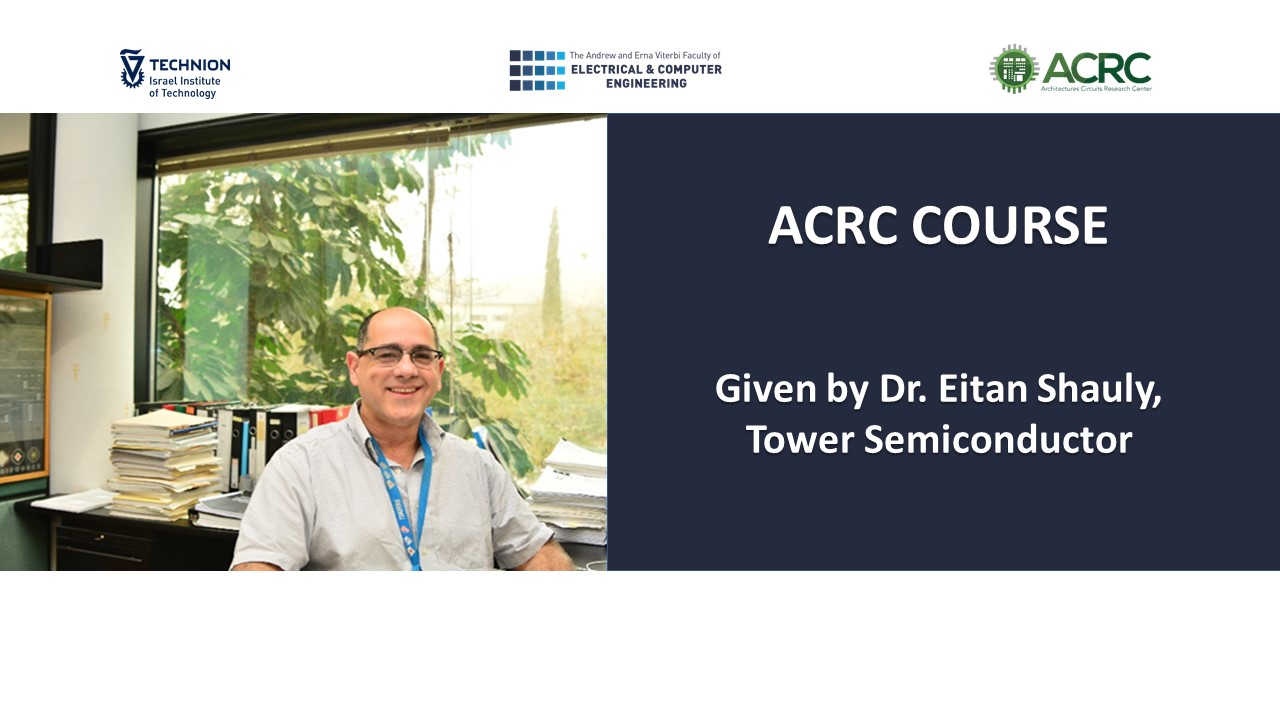
046003 – Reliability of Semiconductor Devices
September 18-20, 2022
Auditorium 280, Mayer Bld.
Dr. Eitan Shauly, Tower Semiconductor
| Instructor: | Dr. Eitan Shauly |
| Teaching assistant: | Efrat Ordan |
| Lectures: | 13 hours, 3 days |
| Academic points: | 1pts |
| Exam: | TBD |
| Course Fee : | 1700$ (see membership options) |
*Registration is open until August 18, 2022
Sylabus:
Detailed overview of reliability failure mechanisms and modeling, from the foundry perspective. Covered Physical and Environmental FEOL and BEOL qualification, Automotive.
Topics:
| 1 | Introduction to Reliability and time degradation
Quality and Reliability; The Reliability bathtub Failure in time and the acceleration factors (Temp, Voltage, Currents stress) MTTF (Mean-time-to-Failure), MTBF (Mean-time-between-Failure), FIT (Failure-in-time) Materials and device degradation vs time – modeling, Competing degradation mechanisms, Definition of quality and reliability; Yield vs Reliability; Reliability Scaling, Physical failure mechanisms (Intro): HCI, NBTI, EM, SM, ESD,; Latchup, Soft error |
| 2 | EM=Electromigration
Introduction-BEOL reliability concerns; Electromigration–definition; Mass motion and flux modeling; Blech length; Void formation; Stress effects EM testing and qualification; Grain Size dependency, Alloys, Barrier metals and other process related performances improvement, N7 and N5 BEOL solutions EM LT as function of Width and length EM under AC vs DC conditions; EM scaling limitations |
| 3 | SM = Stress Migration in solid Materials
Stress migration, void formation and growth Stress migration modeling w/ and w/o dielectric all—around Physics of stress migration; Nucleation; Activation diffusion volume Resistance change due to voids growth, stress gradients SIV = Stress-Induced-Voids SIV modeling; Layout solution, double via solution; Stacked via sensitivity, effect of misalignment BEOL dielectric cracking SM and SIV qualification |
| 4 | HCI=Hot Carrier Injection
Carriers’ mobility; currents and voltages in MOSFET under operation: Vt, Id, Ib, Is, CLM, SCE, DIBL, HCI – mechanism and modeling; DAHC (Drain Avalanche Hot carrier), CHE (Channel hot Electron), SHE (Substrate Hot Electron), others; Lucky Electron Model, Interface charge generation, HCI degradation under worse case conditions in planar MOSFETs and FinFETs, HCI qualification – measurement, analysis and modeling HCI under AC conditions, Process solutions to reduce HCI: DDD, spacer with LDD implant, HALO/Pockets; HCI scaling and integration |
| 5 | NBTI=Negative-Bias-Temperature-Instability,
Degradation Mechanism and modeling; Interface traps; The Reactive-Diffusion (R-D) degradation model, PBTI; Stress time and degradation saturation; NBTI recovery; Dynamic NBTI Qualification and modeling; NBTI Temperature dependency; NBTI Voltage exponential dependency; Voltage/Field acceleration factor Process dependency; Boron Penetration, ; Oxynitridization, DPN; Fluorine passivation, |
| 6 | GOI=Gate Oxide Integrity,
GOX scaling, interfaces, Leakage; Tunneling, TAT, Qbd, Vbd,; Layout sensitivity; Weibull distribution Charge inside GOX, C-V; Vbd; SBD, HBD, TDDB – physical mechanisms, IBM modeling, Process Enhancement GOI Capacitors reliability, with Oxide-Nitride-Oxide, Nitride, Ta2O5; HKMG (Hf-based); TDDB of FinFETs, TDDB – Qualification and Modeling IMD-TDDB |
| 7 | PID=Plasma Induced Damage,
The mechanism of PID; Plasma non-uniformity, shading Degradation of dielectric layers during PID Antenna Ratio: traditional definition; Antenna rules, calculations and examples; Limitation of the traditional ratio; Cumulative plasma damage PID dependency on integration flow; PID dependency on Gate oxide; PID stress and measurement methods, PID structures Protection: bridging, protective diode; Well charging, protection |
| 8 | Environmental qualification and the foundry responsibility
Foundry TQV for platform development; SRAM TEG: structure, scaling, operation, layout Level-2 qualification – Environmental tests · Early Life Failure Rate (ELFR) – calculation · Burin-In for screening · Random failures, x-ray soft error, · High-temperature operating life (HTOL) · Biased temperature and humidity (THB, 85/85) · Temperature cycling (TMCL) · Autoclave |
| 9 | Qualification; The fabless/foundry reliability and qualification “relationship”,
The foundry TQV for qualification and WLR in HVM; Reliability characterization; JEDEC JP001 (1, 2, 3) Examples for foundry physical reliability qual plan and results Additional qualification needs (PID, DRV, CA, Cp/Cpk) |
| 10 | Reliability for Automotive;
IoT, Automotive, connectivity. Examples for different Automotive applications Different qualification requirements for Automotive; Reliability for Automotive; Cumulative failure and life-time The mission profile; AEC-Q100; ZEVI, Environmental qualification and Burn-In Quality and Manufacturing for Automotive; Risk management; IATF16949; The Zero-defect program’ Process Control for Automotive’ Continuance Improvement plan’ 8D report, Failure Analysis capabilities DfA – Design-for-Automotive; Devices, rules, Guidelines and DfM’ SPICE modeling – Aging’ IPs, ISO26262’ ASIL, Safety Function’ Trace and tractability |
| 11 | ESD=Electrostatics Discharge,
ESD and Triboelectric; The (cost) impact of ESD; The level of voltage build-up, examples for failures, ESD Prevention and protection, ESD Modeling; HBM; MM; CDM ESD Protection; example |
References:
- Reliability and Failure of Electronic Materials and Devices, Milton Ohring, Academic Press (1998)
- Reliability Wearout Mechanisms in Advanced CMOS Technology (IEEE Press Series on Microelectronic Systems, Alvin W. Strong et al., John Wiley (2009)
- Up to date list of papers.
Expected Results:
Fulfilling course requirements student is expected to be able to:
- Understand the different reliability mechanisms in CMOS devices,
- Understand the dependencies between the process and the stress conditions in the field on the failure rate
- Fully characterize and analyze the reliability performance and figure of merits of different devices, by carful understanding the different mechanisms and the reliability characterization.
- Deep understanding of the way the semiconductor devices operates under stress (transistors, capacitors, resistors and more) thus how to optimize them to achieve the needed performance, with emphasize on reliability for automotive
Prerequisites:
- 044231 Electron Devices 1 (MOS)
Assignments:
The course will consist of: lectures, self-practice exercises (35% of the grade), and a final exam (65% of the grade).
Course schedule:
| 18-Sep’22 | 1 | 09:00 ~ 09:50 | Course Introduction, Introduction to Reliability and time degradation, (TAF, CAF, VAF), modeling |
| 2 | 10:00 ~ 10:50 | Physical failure mechanisms: HCI, NBTI, EM, SM, GOI, ESD, others | |
| 3 | 11:00 ~ 12:00 | Electromigration: definition; Mass motion and flux modeling; Blech length; Void formation; Stress effects | |
| 4 | 12:00 ~ 13:00 | Lunch Break | |
| 5 | 13:00 ~ 13:50 | Electromigration – testing and qualification; | |
| 6 | 14:00 ~ 15:15 | Electromigration: Grain Size dependency, Alloys, Barrier metals and other process related performances improvement, N7 and N5 BEOL solutions | |
| 7 | 15:30 ~ 17:00 | Electromigration: LT as function of Width and length, AC vs DC conditions; EM scaling limitations. Stress Migration: Introduction |
|
| 8 | 17:10 ~ 18:00 | Stress Migration: void formation and growth; SIV modeling; Layout solution, double via solution; Stacked via sensitivity, effect of misalignment | |
| 19-Sep’22 | 1 | 09:00 ~ 09:50 | Hot-Carrier-Injection: mechanism and modeling; DAHC (Drain Avalanche Hot carrier), CHE (Channel hot Electron), SHE (Substrate Hot Electron), others; Lucky Electron Model, |
| 2 | 10:00 ~ 10:50 | HCI: HCI degradation under worse case conditions in planar MOSFETs and FinFETs, qualification – measurement, analysis and modeling, Process solutions to reduce HCI: DDD, spacer with LDD implant, HALO/Pockets; Aging | |
| 3 | 11:00 ~ 12:00 | Negative-Bias-Temperature-Instability: Degradation Mechanism and modeling; Interface traps; The Reactive-Diffusion (R-D) degradation model, PBTI; | |
| 4 | 12:00 ~ 13:00 | Lunch Break | |
| 5 | 13:00 ~ 13:50 | NBTI: Stress time and degradation saturation; NBTI recovery; Dynamic NBTI; Qualification and modeling; Process dependency; Boron Penetration, ; Oxynitridization, DPN; Fluorine passivation, | |
| 6 | 14:00 ~ 15:15 | Gate Oxide Integrity: GOX scaling, interfaces, Leakage; Tunneling, TAT, Qbd, Vbd,; Layout sensitivity; | |
| 7 | 15:30 ~ 17:00 | GOI: Weibull distribution; Charge inside GOX, C-V; TDDB – physical mechanisms, IBM modeling, | |
| 8 | 17:10 ~ 18:00 | GOI / Tirgol | |
| 20-Sep’22 | 1 | 09:00 ~ 09:50 | GOI: Process Enhancement GOI; Oxide-Nitride-Oxide, Nitride, Ta2O5; HKMG (Hf-based); |
| 2 | 10:00 ~ 10:50 | GOI: TDDB of FinFETs, TDDB – Qualification and Modeling, IMD-TDDB | |
| 3 | 11:00 ~ 12:00 | Plasma Induced Damage: The mechanism of PID; Plasma non-uniformity, shading, Antenna Ratio: traditional definition; Antenna rules, calculations and examples; Limitation of the traditional ratio; Cumulative plasma damage; Protection: bridging, protective diode; Well charging, protection | |
| 4 | 12:00 ~ 13:00 | Lunch Break | |
| 5 | 13:00 ~ 13:50 | Technology qualification: TEG, TQV, ELFR, Burn-In, HTOL, THB, 85/85 | |
| 6 | 14:00 ~ 15:15 | Technology qualification: TMCL, JEDEC JP001 | |
| 7 | 15:30 ~ 17:00 | Automotive: Reliability, AEC-Q100, ZEVI, Mission Profile, Quality, IARF16949, DFA, IPs, ISO 26262 | |
| 8 | 17:10 ~ 18:00 | Electrostatics Discharge: Mechanism, examples for failures, Prevention and protection, HBM, MM, CDM |
Lecturer Bio:
Dr. Eitan N. Shauly received the B.Sc. degree in materials engineering from Ben-Gurion University, Beer-Sheva, Israel, in 1989, and M.Sc. and Ph.D. degrees in materials engineering from the Technicon — Institute of Technology, Haifa, in 1995 and 2001, respectively. He has worked for Tower Semiconductor since 1989. During 1989–1994 he was a diffusion and ion implantation engineer. During 1994–1997 he was a device/Integration engineer, focusing on process integration and process modeling. Since 1998 he is doing integration, focusing on platform development, design rules, Design-for-Manufacturing and Automotive. Dr. Shauly is also teaching at the faculty of Material Engineering, Technicon Haifa, courses related to VLSI technology: “VLSI processing” and “CMOS Devices and Integration”.
*Registration is open until August 18, 2022


